Metal Delamination Analysis Process
Case Study of Electronic Materials Packaging with Poor Metal Adhesion and the Process for Performing Root Cause Failure Analysis
Dr. E. A. Leone
Background
One trend in the electronic packaging industry is to minimize size of components. In order to accomplish this, the dimensions of metal traces must become smaller (10-50 µm), which requires higher resolution of profiles around edges and in vias (holes in the package substrate that provide electrical connections between layers). Another essential requirement is that the metal traces must have excellent adhesion to the polymer substrate, so that detachment does not occur during subsequent wet processing steps.

Figure 1. Optical picture of a patterned wire bond substrate.
A picture of a portion of a micro-electronic package is shown in Figure 1. Each side of the square has dozens of electrical contacts, which are about 50 µm in width. A simplified process for manufacturing the package with major processing steps is shown in Figure 2. The first step in the process is to laser drill vias (holes) through the substrate. After a number of cleaning steps including plasma treatments,the substrates are placed in a vacuum chamber where metal is sputtered onto the film surface. Any of the processing steps prior to metal deposition can have a direct impact on substrate/ metal adhesion. The remaining steps in the process are generally “wet” processing stages, where patterning is performed using standard lithographic techniques. The primary objective of this investigation was to understand the adhesion mechanism of metal to a polyimide substrate, and to improve the level of metal adhesion, which initially was below the level required by customers.

Figure 2. Simplified process of manufacturing a patterned wire bond substrate.
The polymer substrate of choice for this application was a polyimide with the chemical formula shown in Figure 3.
Polyimides have excellent mechanical and electrical properties that make it an attractive material as an interlayer dielectric. In addition, it has good thermal stability, low moisture adsorption, good UV absorption behavior, good chemical resistance and overall easy processability.

Figure 3. Chemical structure of a typical polyimide substrate.

Figure 4. Schematic diagram of metal plated substrate.
In order to get good bonding to the copper traces, an adhesion promoter such as chromium is required. In the metallization process, thin Cr and Cu layers are usually sputtered deposited first. This is followed by deposition of a thicker layer of electroplated copper. A schematic diagram of a typical package is shown in Figure 4. Also indicated in the figure are a number of possible failure modes where de-bonding can occur. Good adhesion is required for these high-density packages that utilize fine-line circuitry, since chemical attack during the wet processing stages can induce degradation of the metal/ polymer interface at line edges. In order to get good adhesion of the metal to the polymer, a surface treatment is usually required. There are two major benefits of the surface treatments: (1) to remove surface contamination and weak polymer layers (low molecular weight, oriented layers, etc.); and (2) to add surface functionality that will bond strongly to the first metallized layer (in this case, chromium).
Results
In performing root cause failure analysis, it is important to fist identify all major factors which can have a direct impact on adhesion. We examined four areas as indicated in Figure 5: (1) material selection; (2) substrate pre-treatments; (3) the sputter deposition process; and (4) plating/ wet chemistry issues. Material selection refers to issues like side-to-side variation, surface composition, dimensional stability and polymer orientation. Typical pre-treatments include solvent washing, plasma and reactive ion etching (RIE). Conditions during sputter depositions are critical, such as temperature, pressure, plating quality, and oxygen content. Also, there are wet plating issues such as thickness, stress, and pinhole formation in the conducting layer.
One of the key issues in the investigation is to quickly determine the active failure modes, as indicated in Figure 4. One of the best analytical methods to determine this is with x-ray photoelectron spectroscopy (XPS). Figure 6 shows XPS survey scans of: (a) the substrate side

Figure 5. Root cause analysis fault tree used to identify cause of poor metal adhesion.
 the polyimide
substrate; and (b) the metal foil. The failure occurred between the polyimide substrate and the first metal layer (chromium)")
Figure 6. XPS spectra showing example of adhesive failure of a peel between: (a) the polyimide substrate; and (b) the metal foil. The failure occurred between the polyimide substrate and the first metal layer (chromium).
of the peel and (b) the metal side. The substrate side is predominately polyimide, while the metal side is chromium. This indicates that the failure mode is adhesive, meaning that the failure is located between the substrate and the sputter deposited chromium layer. The peel strengths of these samples were typically < 1 lb/ in. However, the peel strengths required by customers are > 4 lb/ in. These original substrates were chemically etched and rinsed with water. XPS analysis detected a number of residues left on the surface (e.g. etchant and rinse residues), which accounted for the poor adhesion. Using plasma treatments, with O2 and O2/CF4 plasma compositions, significant improvements in bond strengths were observed. Again, XPS was used to identify oxygen functionality incorporated into the surface consisting of basic groups, such as alcohols and ethers (C-OR), carbonyls (-C=O) and esters (-COOR), which form chemical bonds with the sputter deposited chromium.
In addition to studying the surface chemistry, it was also important to measure changes in surface roughness and morphology using atomic force microscopy (AFM). AFM pictures, before and after O2/ CF4 plasma treatments are shown in Figure 7. From the AFM measurements, one can measure surface roughness. After treatments, tiny particles were observed at the surface. We believe that these were polymer “anti-block” particles buried just under the surface, which were exposed after removal of a layer of polymer skin by the plasma. Other treatments included reactive ion etching (RIE) which was found to incorporate even higher levels of oxygen functionality into the surface. Figure 8 shows XPS plots of oxygen concentration versus surface treatment. We found that RIE methods created maximum oxygen functionality at the surface of the polyimide film. These treatments also affected surface energy components, which is indicated in Figure 9. One interesting finding was that the surface
 before; and (b) after plasma treatment. The treatment revealed anitblock particles buried in the film (red spots).")
Figure 7. AFM analysis of CF4 / O2 plasma treated polyimide film: (a) before; and (b) after plasma treatment. The treatment revealed anitblock particles buried in the film (red spots).

Figure 8. XPS analysis of polyimide substrates with different treatments, comparing surface oxygen concentrations.
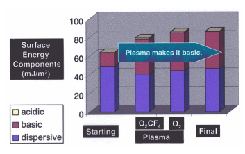
Figure 9. Surface energy measurements of treated polyimide substrates showing how physiochemical reactions can
increase the surface basic component of the total surface energy measurement.
treatments accelerated the growth of basic components at the surface. This is supported by the XPS data, which also revealed basic species at the surface.
A chart displaying the progress made during the 6 month time period of the investigation is shown in Figure 10. Customers required peel strengths at least 3-6 lb/in. Using oxygen plasma treatments we were able to significantly increase the peel strengths. As the peel strengths increased, it was noted that the failure mode measured by XPS became more cohesive, with failure occurring within the polyimide substrate. The final improvement, which exceeded Customer expectations, was made through modifications of the sputtering unit to perform in-situ RIE treatments. RIE provided a highly activated surface that interacted strongly with the sputter deposited chromium, creating high peel strengths and ultimate failure in the polymer substrate.
Summary and Conclusions
.")
Figure 10. Progress in optimizing surface chemistry improvements and metal/ substrate adhesion (peel strengths).
The first step in the root cause failure analysis is to establish a fault tree with all possible failure modes, and identify analytical methods to characterize the potential faults. One of the initial tasks is to determine the failure mode (i.e., the location of the weakest interface). In the study, XPS clearly determined that the low peel strengths were associated with adhesive failures between the polymer substrate and the sputter deposited chromium layer. Other analytical techniques can be used depending upon analysis depth ToF-SIMS (10 Å), XPS (100 Å), SEM or FTIR (1 µm). Multiple analytical techniques may be required. For this study, we used XPS, AES, ToF-SIMS, FTIR, SEM, AFM, surface energy, XRD and mechanical testing.
In this investigation, we found that appropriate substrate pre-treatments can eliminate polymer surface orientation and contamination, and increase oxygen functionality and adhesion to metal layers. The benefits of plasma and RIE treatments are:
- Activation of the surface by increasing surface oxygen functionality.
- Promoting increased chemical bonding to sputtered metals (chromium).
- Reacting with surface oxygen species carbonyls (C=O) and π-complexes.
- Increasing the surface energy and basic functionality.
- Roughening of the surface, which serves to increase the surface area and mechanical interlocking.